Olivier Courtois Design offers a rich and diverse expertise that covers the different stages of a product design. Restricting ourselves to a specific role has never been our philosophy. Our focus is on overcoming challenges and delivering solutions! Thus, OCd extends it’s fruitful contribution wherever it’s needed to get the job done.
PCB Design ++
A PCB Designer that helps you go beyond!
OCd Brings Solutions into your Reality !
PCB LAYOUT ++
Olivier Courtois Design offers a PCB layout focused service, along with active engineering services. Working in efficient collaboration with your in-house resources, OCd delivers beyond expectations results and solutions !
We offer flexible and customizable services. OCd can take charge of the PCBA fabrication and testing, delivering a turn-key solution for any kind of production volume.
We can also reduce the design cost by working in close collaboration with your engineering team and your preferred PCB vendor to efficiently handover the design. Thus, the technical knowledge and expertise stay within your company, granting you complete independence moving forward. Our availability and care characterize post-delivery services !
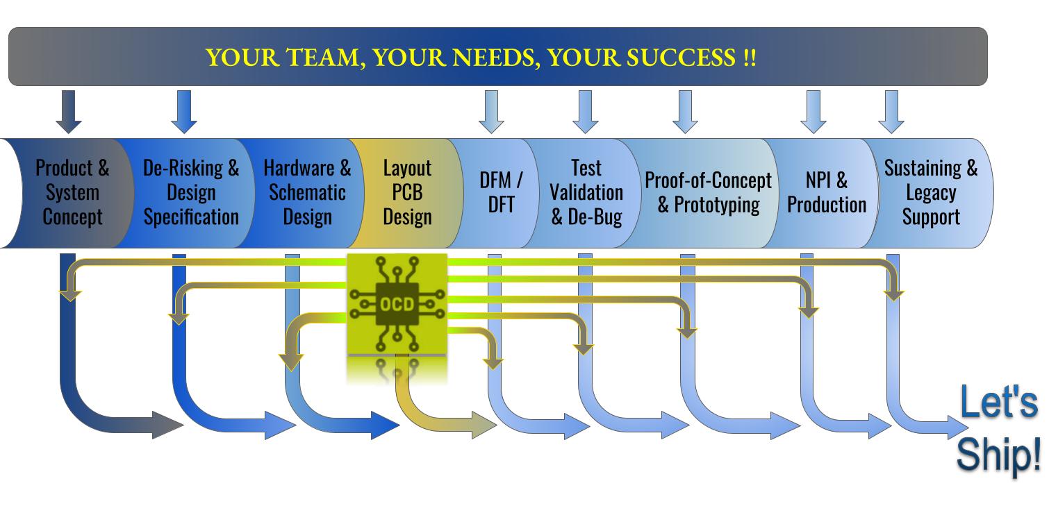
As an experienced electronic engineer, Olivier Courtois Design covers the various stages of an electronic product development (see details below). Been solution driven, OCd covers and address challenges regardless of the discipline. We get the job done !
We usually work with Altium Designer. We can work with and enrich your own library or we can adapt and create a new one that fits your current and future needs.
COMPLETE PCB DESIGN: SCHEMATIC AND LAYOUT ++
In this option, you’ll be provided with the full potential of our skills set. Olivier Courtois Design covers the various stages of a product design.
Our solutions offer peace of mind by taking charge of the electronic design activities, so you may focus your time and energy on other aspects of your business. We deliver a turn-key PCB solution tailored to your reality and your needs ! Our clients are provided with the best compromise between features, quality, “time-to-delivery”, and cost ! Whether it’s a prototype or a high-volume production, we got you covered!
Our communications are simple and efficient, minimizing the impact on your in-house resources. Because of our engineering background, we understands your reality !
Teaming with Olivier Courtois Design frees you from the electronic related headaches. Our availability and care characterize our post-delivery services !
Been solution driven, OCd covers and address challenges regardless of the discipline. We get the job done !
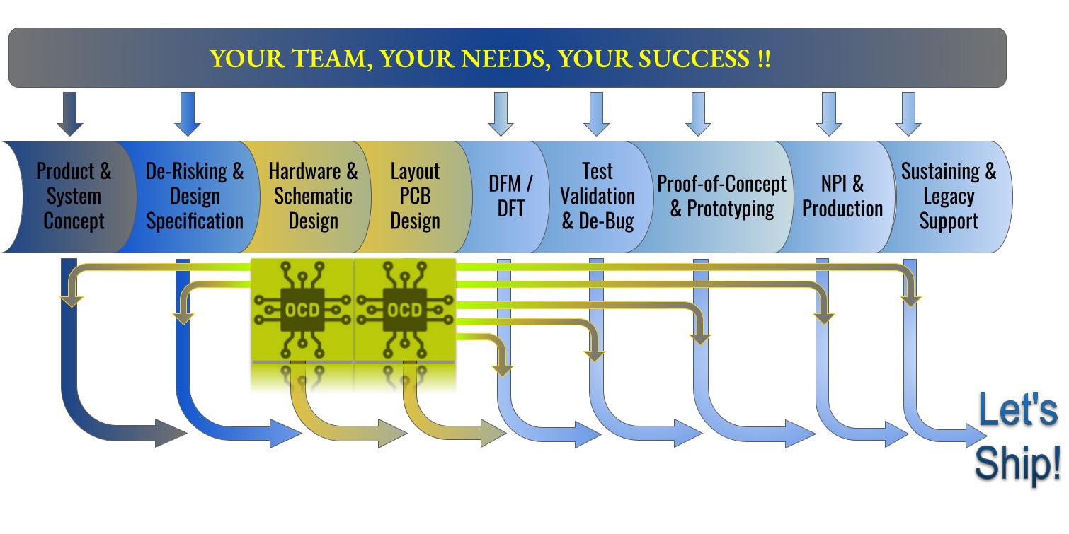
Product & System Concept
Product & System Concept
- Product Specifications
- System level Specifications
- Form Factor/Assembly Structure
- Interface Definition
- Firmware/Software Platform
De-Risking Assessment & Hardware Design Specifications
De-Risking Assessment & Hardware Design Specifications
- Critical Parts Assessments
- Hardware Features
- Firm/Soft De-Risking
- MEC constraints
Hardware & Schematic Design
Hardware & Schematic Design
- Schematic Circuit Design
- Procurement Assessments
- BOMs
- Test Plans
PCB Design Layout
PCB Design Layout
- PCBA Design Layout
- MEC Constaints
- Form Factor
- Interfaces
- EMI & Noise Control
- Product Assembly
- DFx
DFM / DFT
DFM / DFT
- PCBA Array Optimization
- Design for Certification
- Mass Production Scalability
- Minimize Vendor Back & Forth
- Quick Turn-Over
- Test Features for PCBA Vendor
- Test Features for Production Testing
- Test Features for Prog. & Debug
Test Validation & De-Bugging
Test Validation & De-Bugging
- Bring-Ups!
- Qualification Tests
- Functionality Tests
- Certification Tests
- Product and System Spec. Validation
- De-Bugging!
Proof-of-Concept and Prototyping
Proof-of-Concept and Prototyping
- Fast Design, Fast Answers!
- Low Volume
- Feature Testability
- Feature Functionnality
NPI & Production
NPI & Production
- Assembly + Testing SOPs
- Testing and Prog. Jig
- Transfert to Production Ing.
- Cost Reduction
- Vendor Assessments
- Production Optimization
Sustaining & Legacy Support
Sustaining & Legacy Support
- Component Engineering
- End-of-Life Components
- Re-Design
- Customization
- Cost Reduction
List of abbreviations
OCd: Olivier Courtois Design
PCB: Printed Circuit Board
PCBA: Printed Circuit Board Assembly
DFM: Design for Manufacturing
DFT: Design for Testing
DFx: Inclusive of all Design For ….
NPI: New Product Introduction
BOM: Bill of Material
MEC: Mechanical
EMI: ElectroMagnetic Interference
SOP: Standard Operating Procedure
Glossary
*** Definitions may vary from one company to another ***
Schematic Design: Design of the electronic circuit drawings.
Layout Design: Creation of the Printed Circuit Board. Materialization of the electronic circuit drawings.
Lead Designer : Person responsible for conducting all the activities around the development of the electronic product. Discipline implication may vary.
Schematic designer: Person responsible for the schematic design. Might also play the role of the Lead Designer.
Prime Designer: Similar to Lead Designer.