Olivier Courtois Design offers a rich and diverse expertise that covers the different stages of a product design. Restricting ourselves to a specific role has never been our philosophy. Our focus is on overcoming challenges and delivering solutions! Thus, OCd extends it’s fruitful contribution wherever it’s needed to get the job done.
On Demand Resource !
An Electronic Engineer resource where It’s most needed !
You’re in need of an additional resource for your important project ?
You are not able to fill the open position and the schedule keeps slipping ?
Our affordable services add the extra hands you need to meet your delivery dates !
Specialized in PCB Layout Design, OCd provides the same experience and expertise wherever you need it !
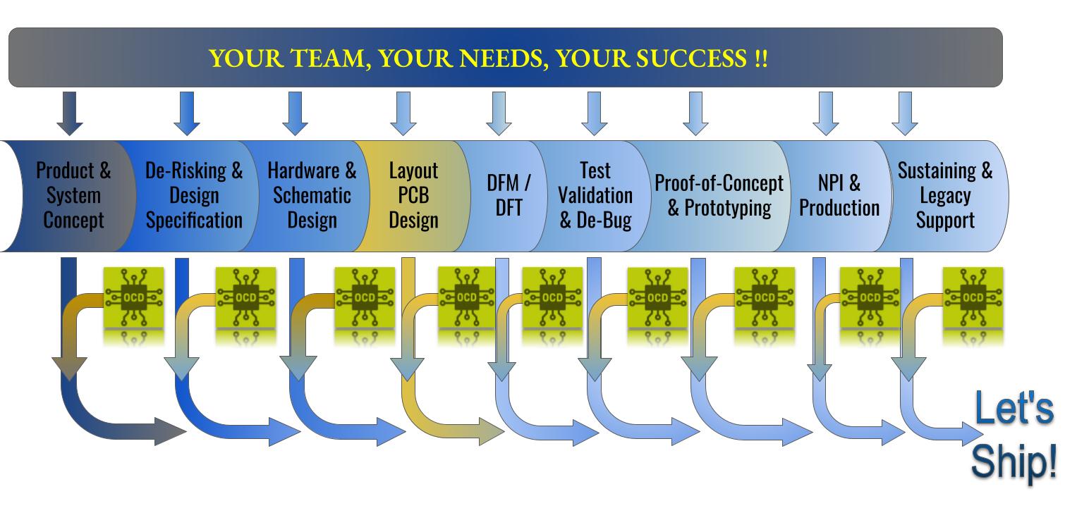
Product & System Concept
Product & System Concept
- Product Specifications
- System level Specifications
- Form Factor/Assembly Structure
- Interface Definition
- Firmware/Software Platform
De-Risking Assessment & Hardware Design Specifications
De-Risking Assessment & Hardware Design Specifications
- Critical Parts Assessments
- Hardware Features
- Firm/Soft De-Risking
- MEC constraints
Hardware & Schematic Design
Hardware & Schematic Design
- Schematic Circuit Design
- Procurement Assessments
- BOMs
- Test Plans
PCB Design Layout
PCB Design Layout
- PCBA Design Layout
- MEC Constaints
- Form Factor
- Interfaces
- EMI & Noise Control
- Product Assembly
- DFx
DFM / DFT
DFM / DFT
- PCBA Array Optimization
- Design for Certification
- Mass Production Scalability
- Minimize Vendor Back & Forth
- Quick Turn-Over
- Test Features for PCBA Vendor
- Test Features for Production Testing
- Test Features for Prog. & Debug
Test Validation & De-Bugging
Test Validation & De-Bugging
- Bring-Ups!
- Qualification Tests
- Functionality Tests
- Certification Tests
- Product and System Spec. Validation
- De-Bugging!
Proof-of-Concept and Prototyping
Proof-of-Concept and Prototyping
- Fast Design, Fast Answers!
- Low Volume
- Feature Testability
- Feature Functionnality
NPI & Production
NPI & Production
- Assembly + Testing SOPs
- Testing and Prog. Jig
- Transfert to Production Ing.
- Cost Reduction
- Vendor Assessments
- Production Optimization
Sustaining & Legacy Support
Sustaining & Legacy Support
- Component Engineering
- End-of-Life Components
- Re-Design
- Customization
- Cost Reduction
List of abbreviations
OCd: Olivier Courtois Design
PCB: Printed Circuit Board
PCBA: Printed Circuit Board Assembly
DFM: Design for Manufacturing
DFT: Design for Testing
DFx: Inclusive of all Design For ….
NPI: New Product Introduction
BOM: Bill of Material
MEC: Mechanical
EMI: ElectroMagnetic Interference
SOP: Standard Operating Procedure
Glossary
*** Definitions may vary from one company to another ***
Schematic Design: Design of the electronic circuit drawings.
Layout Design: Creation of the Printed Circuit Board. Materialization of the electronic circuit drawings.
Lead Designer : Person responsible for conducting all the activities around the development of the electronic product. Discipline implication may vary.
Schematic designer: Person responsible for the schematic design. Might also play the role of the Lead Designer.
Prime Designer: Similar to Lead Designer.